TM 11-5840--281-35/1
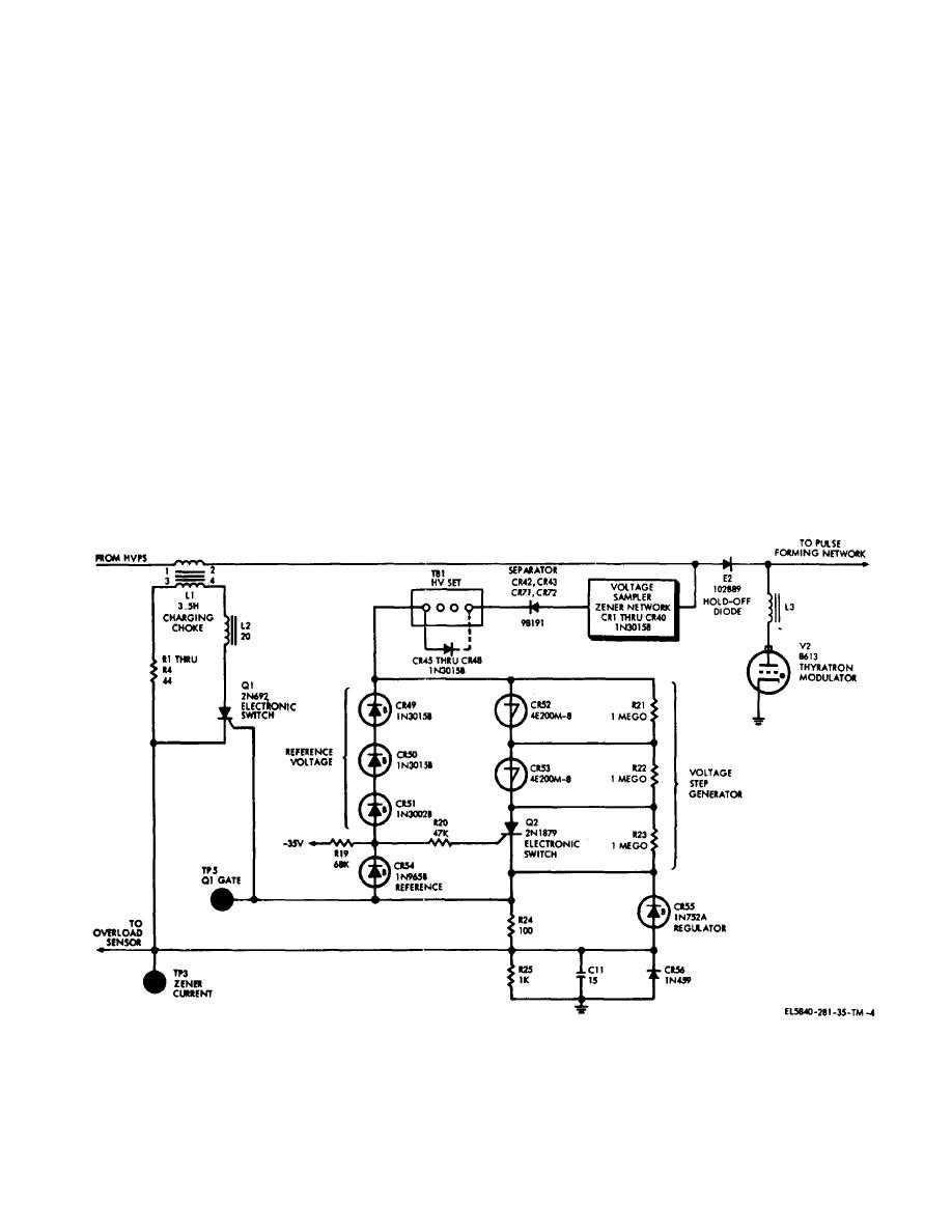
con-controlled rectifier Q202 is a value of 0.3 ma.
excess power. The sudden current surge caused by the
With silicon-controlled rectifier 202 turned on, the total
breakdown of silicon-controlled rectifier Q202, diodes
475 volts is placed across resistors R221 and R222,
CR252 and CR253, develops a voltage across resistor
overcoming the required breakdown potential of four
R224 which is applied to silicon-controlled rectifier Q201
layer diodes CR252 and CR253.
gate to initiate Q201 Conduction. Diode CR255 limits
The conduction of silicon-controlled rectifier Q202 and
silicon-controlled rectifier Q201 gate voltage to 5.6 volts.
diodes CR252 and CR253 shorts the +475-volt pulse
When silicon-controlled rectifier Q201 conducts, resistors
developed across diodes CR249, CR250, and CR 251.
R201 through R204 are connected across charging
When this occurs, Zener net- work diodes CR201
choke L201 secondary to absorb the excess energy
through CR240 see a 475-volt change at the low-voltage
stored in the charging choke field. The volt- age across
end and must produce a similar range at the high-voltage
resistor R225 developed by the Zener current is held to a
end since the network voltage drop remains essentially
nominal value by the discharge of capacitor C211
constant. The sudden decrease in voltage at the
through resistor R225 as a result of the long time
junction of charging choke L201 and hold-off diode E202
constant. The voltage represents the average Zener
reverse-biases E202, disconnecting pulse-forming
current in milliam- peres as measured at test point
network Z201 from the resonant charging circuit. Pulse-
TP203. In case of excessive Zener current, the resulting
forming network Z201 well then be charged to the same
voltage across resistor R225 and capacitor C211 is
reference voltage on each successive pulse, regardless
applied to transistor Q204 in the overload sensor circuit.
of line voltage changes.
(3) The backswing (reverse current) circuit of the
(2) Since the Zener network is not capable of
high-voltage regulator (fig.2-5) protects the modulator
dissipating all of the energy stored in the field of charging
circuit from breakdown. If the magnetron begins to arc
choke L201, an auxiliary circuit, consisting of silicon-
excessively, the pulse forming network is then
controlled rectifier Q201 and resistors R201, R203,
terminated into a lead which is less than its characteristic
R203, and R204, absorbs the
Figure 2-4. High voltage regulator circuit, simplified schematic
2-6


 Previous Page
