TM 11-5841-287-30
data to be transmitted downlink with the video data
accomplished as previously described for RAM
During the video write mode, video accumulator address
operation, except signals BA, A15, A11 and M10 (in
signals RAO through RA10 are selected for application
combination) perform the function of signal OXXX These
to the RAM For writing the remaining variable data into
same signals are also used for generation of the ROM
memory, addressing Is performed under MPU control
enable, which goes low to allow access to the ROM
using MPU address lines AO through A10 For purposes
contents by the data bus transceivers
of address selector control, signal BA transitions high
during the video write mode and low for MPU controlled
2-15. Output Format Generator and Receive
writing
Register Sections
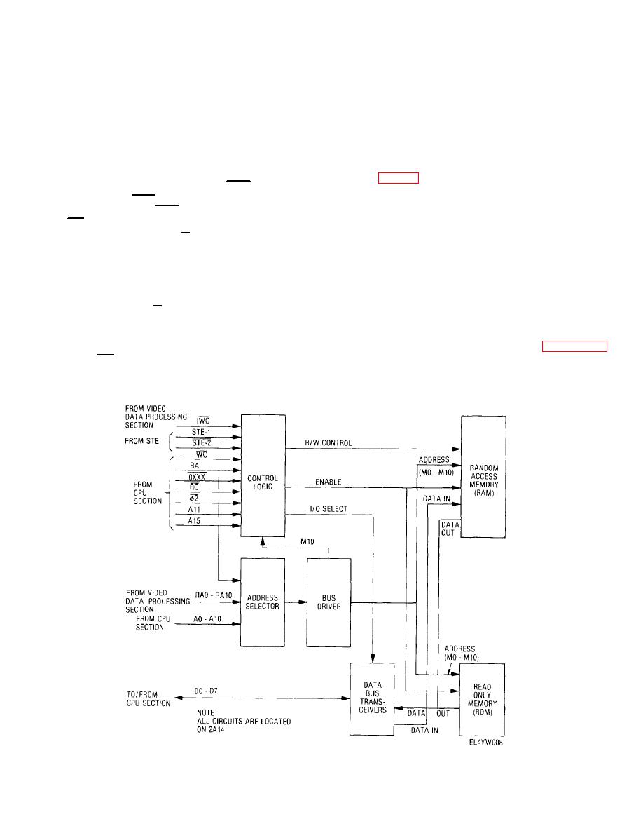
d. Read/Write Control Read/write control of
the RAM is accomplished by signals IWC (integrator
a. Output Format Generator
write control) and WC, which transition low during
(1) General The function of the output
respective write periods IWC is used for video writing,
while WC is used for MPU controlled writing Control of
and video data into final format for transmission down-
the RAM is enabled by signals 2, BA, and OXXX from
link During the final processing, sequence data is serially
the CPU section and M10 from the bus driver For
outputted in groups of two 8-bit parallel words, under
reading data out of RAM, low or high M10 and low OXXX
CPU control Following transmission of each two-word
or BA combine to produce a low level on the RAM enable
data group, an interrupt request (XMIT REG) is
line Inhibiting of the RAM outputs, as represented by a
generated, at which time the next two 8-bit words In
high level on the enable line, occurs during the period
sequence are fetched by the CPU micro-processor and
signal 2 is high and BA is low This allows other sources
placed on the data bus for final processing The
to output data onto the data bus free of RAM interference
sequence is repeated untill all data words have been
Reading MPU program code out of ROM is enabled
transmitted The output format generator circuitry is
(under CPU control) by input signals BA, RC, A15, All
located on output buffer module 2A12 Figure 2-11
and locally derived signal M10 Addressing is provided by
provides block diagram details
input signals AO through A10 During ROM operations,
directional control of the data bus transceiver is
Figure 2-10. Output memory functional block diagram.
2-16


 Previous Page
