TM 11-5841-287-30
FILM SPEED falling edge transitions After the counter
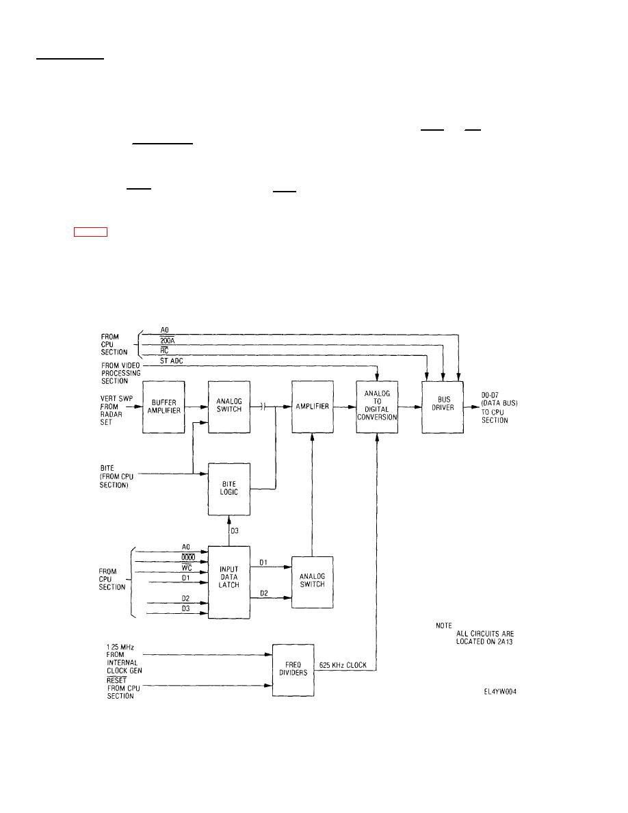
signal generated by the radar set Following buffering and
has been read, D5 goes low, which restarts the control
input switch selection, the VERT SWP input signal is
logic and counter Then D5 returns high to enable the
differentiated and then amplified The ampliflcation factor
next ground speed sample cycle
is controllable and depends upon range and antenna
c. Ground Speed BITE During BITE operation,
mode Control is accomplished in conjunction with
operation of the Input data latch and analog switch Input
high level DO data is applied to the data selector, thereby
signals AO, 0000 and WC are used for clocking-in data
substituting a fixed rate test signal (83 Hz) in place of the
bits D1 and D2, which regulate the amplifier gain via the
FILM SPEED signal The resultant output data words are
analog switch Maximum gain results when the data bits
then checked by the CPU against high and low limit
are high, while minimum gain occurs when both data bits
references stored m the output memory ROM Clocking
are low In voltage terms, the amplifier output is scaled to
of the DO and D5 data through the in-put data latch is
provide a maximum swing of t V for a given input
enabled by signals 0002 and WC
Following amplification, the vertical sweep signal
undergoes analog to-digital conversion to the system 8-
2-11.
Drift Angle Input Data Processing Section
bit word format The A/D conversion rate of 64
microseconds is based on a clock frequency of 625 kHz
a
General The function of the drift angle Input
The 625 kHz, in turn, is derived by dividing a 1 25 MHz
data processing circuitry is to convert drift angle input
input clock by two The A/D converter is enabled by signal
signals received from the recorder to 8-bit parallel format
ST ADC Following analog-to-digital conversion, the eight
for transfer to the output memory section The circuitry is
bits of
located on power fault detector module 2A13
b
Functional Description Aircraft drift angle is
computed by measuring the slope of the vertical sweep
Figure 2-8. Drift angle input data processing functional block diagram.
2-12


 Previous Page
