TM 11-5841-287-30
data undergo transfer to the data bus via the output bus
accomplished (under program control) using the gated
driver which is enabled by signals RC, 200A and AO The
resultant of CPU signals AO, 2008 and RC (read
1 25 MHz frequency divider is started by the RESET
command) to enable the gated bus driver Output data
signal from the CPU section
signals DO through D5 represent range delay, while the
c
Drift Angle BITE During BITE operation
combination of D6 and D7 represent range Once present
on the data bus the range and range delay data
simulated vertical sweep data is generated by the BITE
undergoes processing by the CPU for storage in the
logic BITE operation commences when the BITE in-put
output memory
line transitions high, at which time the input analog
switch is open-clrculted with respect to the VERT SWP
signal At the same time, test signals are substituted in
2-13.
Central Processing Unit(CPU) Section
place of the VERT SWP signal Test signal magnitude is
generated as a function of data bit D3 When D3 is low, a
a. General The function of the CPU is to
+ 5V level IS applied to the amplifier stage, while a - 5V
execute the operational programs associated with
level is applied when D3 transitions high Circuit
transfer, storage, and outputting of the digitized radar
performance verification is based on comparison of the
data The various operational programs executed by the
output data to reference data stored In output ROM for
CPU are stored m permanent memories (ROM) located
three gain/input level conditions
in the output memory section The circuitry comprising
the central processing unit is located on MPU/timing
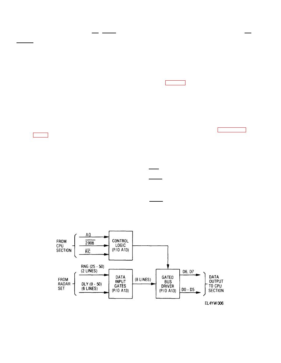
2-12. Range and Range Delay Input Data
module 2All, output buffer 2A12, power fault detector
Processing Section
2A13, and ADAS control 2A16 Figure FO-3 provides
block diagrams
a.
General The function of the range and
b. Microprocessor The primary functional
range delay input data processing circuitry is to convert
element in the CPU is the microprocessor (MPU), which
the range and range delay signals received from the
is abdirectional, bus-oriented 8-bit (DO-D7) parallel
radar set signal processor to 8-bit parallel format for
device, with 16 bit (AO-A15) address capability MPU
transfer to output memory The circuitry, which consists
operation is enabled in conjunction with the following
basically of data input buffers, a data bus driver, and
timing and control functions:
associated control logic, is located on power fault
XTAL.--This input serves as the basic unit clock for the
detector module 2A13
microprocessor
b. Functional Description Range information is
HALT-When
this
input
transitions
low,
the
microprocessor is disabled to allow use of the data bus
received on the RNG (25-50) lines Range selection is
by the video data processing section for purposes of
indicated by high level transition of the corresponding line
transferring MT and FT target data to the output memory
A combination of both lines going low represents 100 km
RESET-This output is generated by the power-on reset
range Range delay information is received on the six
circuit for purposes of starting various functional circuits
DLY (0-50) lines, which go high (individually) to indicate
within the encoder BA-This output signal (normally low)
respective range delay A combination of all range delay
transitions high to indicate that the microprocessor is
lines going low represents 60 km range delay Reading in
disabled
of the range and range delay data is
Figure 2-9. Range and range delay input data processing functional block diagram.
2-13


 Previous Page
