TM 11-5841-287-30
substituted m place of the normal (externally derived)
MODE level has no meaning A low level during a valid
gated 5 MHz clock
sample period indicates the next block of ADAS data will
be in BCD form, while a high level indicates numeric
ADAS data In any case, whichever level is present on the
2-9.
ADAS Input Data Processing Section
MODE line is clocked onto the BCD MODE line when the
ADAS CLOCK signal transitions high.
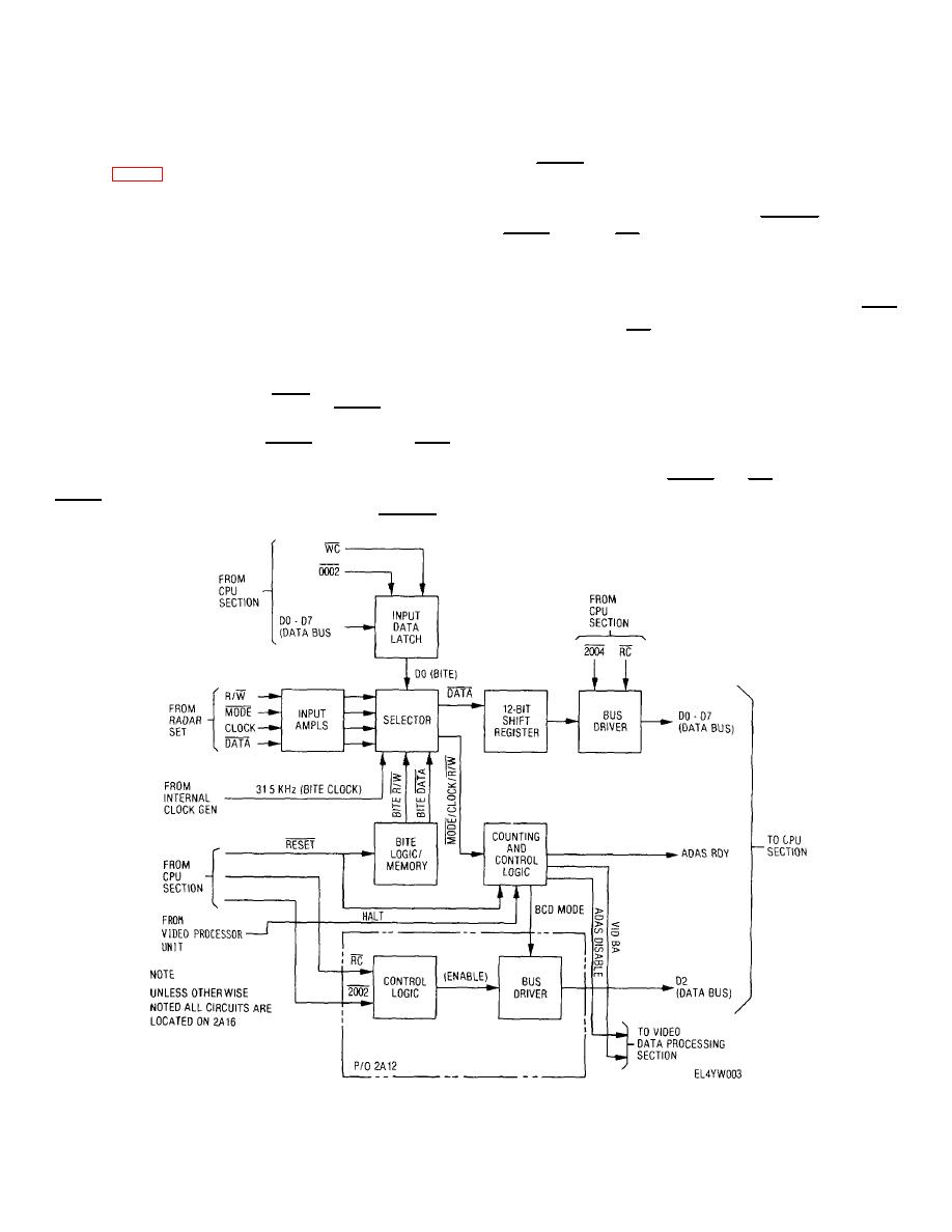
a. General The function of the ADAS input
b. Functional Description Following initial
data processing circuitry is to convert the ADAS data to 8
amplification, the ADAS signals (DATA, CLOCK, MODE
bit parallel format for transfer to the output memory
and R/W) are applied to a selector stage together with
section The circuitry is located on ADAS control module
respective BITE equivalents The level on the BCD
2A16 and output buffer module 2A12 Selector operation
MODE line, in turn, is transferred to the data bus as D2
is controlled by the DO output of the input data latch,
data Enabling of the respective bus driver takes place
which transitions low during normal operation, thereby
during low level coincidence of signals 2002 and RC
selecting ADAS input data from the radar set Following
Counting of the ADAS data bits (for determination of
selection of the airborne or downlink BITE test mode by
word length) commences upon positive transition of the
the operator, DO transitions high, thereby selecting
R/W input signal (prior to such time the ADAS CLOCK
simulated ADAS data generated by the encoder BITE
pulse counting is inhibited) After loading one ADAS data
circuitry Clocking of the input data latch occurs on the
word (8-bits) and four unused parity bits into the 12-bit
negative transition of signals WC and 0002 From the
serial register, the ADAS RDY line transitions high to
data selector, the ADAS data bits are accumulated m a
notify the CPU section that ADAS data is ready for
12-bit shift register, while the MODE, CLOCK and R/W
processing into memory In response to the ADAS ready
signals are routed to various counting and control
interrupt, signal hnes 2004 and RC transition low to
circuitry During certain valid sample periods, the level of
transfer the 8-bit ADAS
MODE indicates whether the next block of ADAS data
will be m BCD or numeric form At all other times the
Figure 2-6. ADAS input data processing functional block diagram.
2-10


 Previous Page
